Introduction
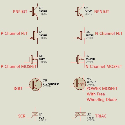
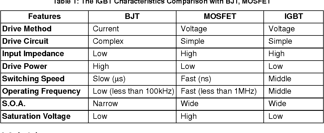
Historically, bipolar semiconductor devices (i.e, diode, transistor, thyristor, thyristor, GTO etc) have been the front runners in the quest for an ideal power electronic switch. Ever since the invention of the transistor, the development of solid-state switches with increased power handling capability has been of interest for expending the application of these devices. The BJT and the GTO thyristor have been developed over the past 30 years to serve the need of the power electronic industry. Their primary advantage over the thyristors have been the superior switching speed and the ability to interrupt the current without reversal of the device voltage. All bipolar devices, however, suffer from a common set of disadvantages, namely, (i) limited switching speed due to considerable redistribution of minority charge carriers associated with every switching operation; (ii) relatively large control power requirement which complicates the control circuit design. Besides, bipolar devices can not be paralleled easily. The reliance of the power electronics industry upon bipolar devices was challenged by the introduction of a new MOS gate controlled power device technology in the 1980s. The power MOS field effect transistor (MOSFET) evolved from the MOS integrated circuit technology. The new device promised extremely low input power levels and no inherent limitation to the switching speed. Thus, it opened up the possibility of increasing the operating frequency in power electronic systems resulting in reduction in size and weight. The initial claims of infinite current gain for the power MOSFET were, however, diluted by the need to design the gate drive circuit to account for the pulse currents required to charge and discharge the high input capacitance of these devices. At high frequency of operation the required gate drive power becomes substantial. MOSFETs also have comparatively higher on state resistance per unit area of the device cross section which increases with the blocking voltage rating of the device. Consequently, the use of MOSFET has been restricted to low voltage (less than about 500 volts) applications where the ON state resistance reaches acceptable values. Inherently fast switching speed of these devices can be effectively utilized to increase the switching frequency beyond several hundred kHz. From the point of view of the operating principle a MOSFET is a voltage controlled majority carrier device. As the name suggests, movement of majority carriers in a MOSFET is controlled by the voltage applied on the control electrode (called gate) which is insulated by a thin metal oxide layer from the bulk semiconductor body. The electric field produced by the gate voltage modulate the conductivity of the semiconductor material in the region between the main current carrying terminals called the Drain (D) and the Source (S). Power MOSFETs, just like their integrated circuit counterpart, can be of two types (i) depletion type and (ii) enhancement type. Both of these can be either n- channel type or p-channel type depending on the nature of the bulk semiconductor. Fig 6.1 (a) shows the circuit symbol of these four types of MOSFETs along with their drain current vs gate-source voltage characteristics (transfer characteristics).
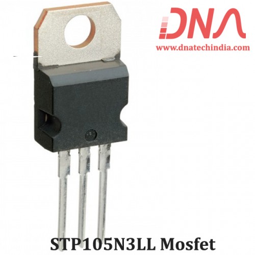
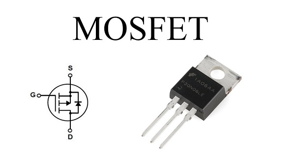
MOSFET IMAGE.


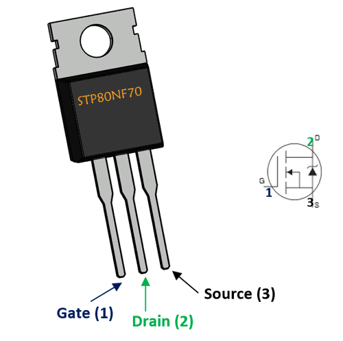
PINOUT IMAGE MOSFET DOWN IMAGE.

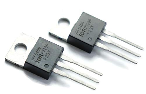
GENERAL IMAGE MOSFET.


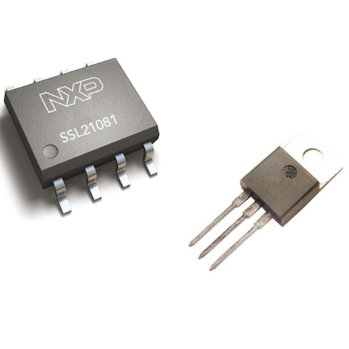
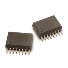
OPTOCOUPLER TRANSSISTOR.


MOSFET NOTES
Metal-Oxide Semiconductor Field-Effect Transistor (MOSFET)
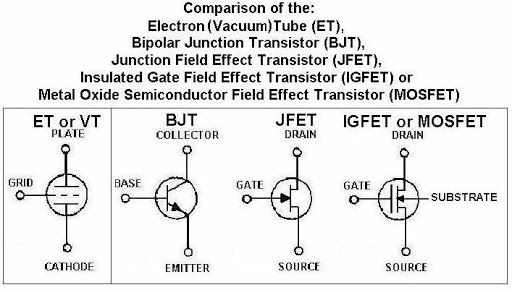
The metal-oxide semiconductor field-effect transistor (MOSFET) is actually a four-terminal device. In addition to the drain, gate and source, there is a substrate, or body, contact. Generally, for practical applications, the substrate is connected to the source terminal. If this is the case (and it usually is), the MOSFET may be considered a standard three-terminal device, with the drain, gate and source the terminals of interest.
Like all FET structures, the MOSFET uses the field effect to operate the attraction or repulsion of charge carriers through an applied voltage but this device has a twist that has allowed it to become the predominant technology for silicon based FETs. The MOSFET structure has dominated primarily due to the availability of a high quality oxide (SiO2, or silicon dioxide) for the silicon system. As we will see, this oxide acts as an insulator and provides electrical isolation between the gate and an active (conduction) channel between the source and drain, thus providing the required input/output isolation.
Now, we get into an interesting part
as you go through this next segment, keep in mind that its okay to share your head in bewilderment initially and that we will be going into detail about all this!
Recall back to our discussion of BJTs and the definition of the two possible flavors that depended on device construction and bipolar operation:
- the npn BJT, where electrons are the majority carrier and holes are the minority carrier; and
- the pnp BJT, where holes are the majority carrier and electrons are the minority carrier.
As mentioned above in our discussion of JFETs, we have the same sort of situation with FETs, but now we only have to define the device in terms of a majority carrier type (unipolar operation). Specifically for MOSFETS we have:
- the n-channel MOSFET, called the NMOS, where the majority carrier type is electrons; and
- the p-channel MOSFET, or PMOS, where the majority carrier type is holes.
Okay, thats pretty reasonable. But
for MOSFETs (and some other FET structures) there is another twist. Due to the insulator layer that exists
